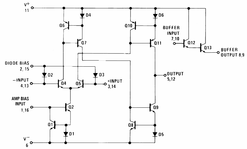
Straight from the datasheet, page 9
When you’re designing a stereo (or more) hi-fi amplifier (which may not be as hi-fi as others, but at least it’s mine !), one of the earlier problems is controlling the volume. And for this, you have multiple options:
OK, so what is an OTA in the first place ? OTA stands for Operational Transconductance Amplifier, which is a fancy word to say that it takes a differential voltage on its input, and outputs a current proportional to this voltage difference. But how does this help us ?
Well, the thing with OTAs is that the current outputs is also proportional to the bias current, which is basically the current that passes through the circuit while it’s idling. If we get an OTA with a bias current we can control, down to zero if possible, we get an amplifier with a variable gain, which is exactly what we want !
Like a normal operational amplifier (which is basically is, but even simpler), an OTA is made of three parts, sometimes more if you want compensation and all the fancy stuff:
Let’s analyze the LM13700’s circuitry to find those !
The bias circuitry is made of Q1, Q2 and D1. A diode here can be seen like a BJT transistor with its base connected to its collector (don’t believe me ? Try in LTSpice :p ). So D1 and Q1 are basically a current mirror. Q2 is here mostly to fix the bias point. The goal here is to have a current flowing through Q2 that is (almost) equal to the current input through pin 1 (AMP BIAS INPUT).
The differential pair is made of Q4 and Q5. As you might see they’re BJT, which means that there will be a current flowing through each input, proportional to the bias current (about 1/400th of it). Keep that in mind for later.
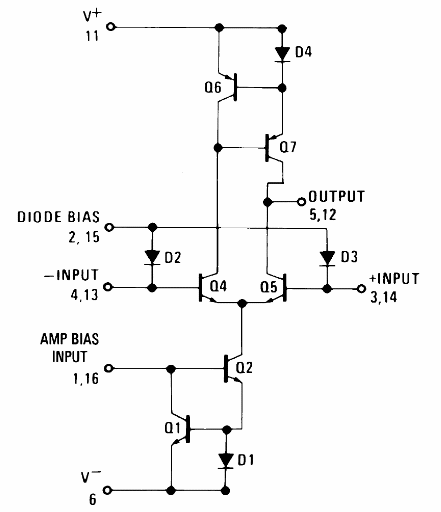
Finally, Q6, Q7 and D4 form the current mirror (note: Q7 makes it almost a cascode, and one could put another transistor to make a complete one, but as the output is single-ended, it doesn’t make much difference). Let’s just no care about the right side with Q9-Q11 and D5-D6, as far as we’re concerned they’re just here as an offset-correcting output stage (and fail spectacularly by the way). And Q12-Q13 is just a bigger buffer, I mean it’s literally written next to it. You can just ignore them, and get the following circuit:
By the way, I know I haven’t talked about D2 and D3, but they’re just here to attempt to compensate for the non-linearity and current sinking of the input transistors. They’ll be ignored from now.
So that’s basically the LM13700. It will do the job as a bias-adjustable OTA, but it’s ancient and is generally criticized for its high distortion (-60dB THD, 0,1%) and noise. So I made it better !
The first obvious way to improve this design is to replace the differential pair transistors by MOSFETs, so that the input current drops from 10th of µA to a few nA.
The current mirror can also be improved in the same way, and as a bonus, the temperature sensitivity is greatly improved !
Finally, the bias circuitry, with no base current on Q2, will be even more accurate. And let’s replace all diodes with transistors too, to reduce the different part count (and make it cheaper !).
As I’m a big fan of LTSpice, I built this exact circuit in it:
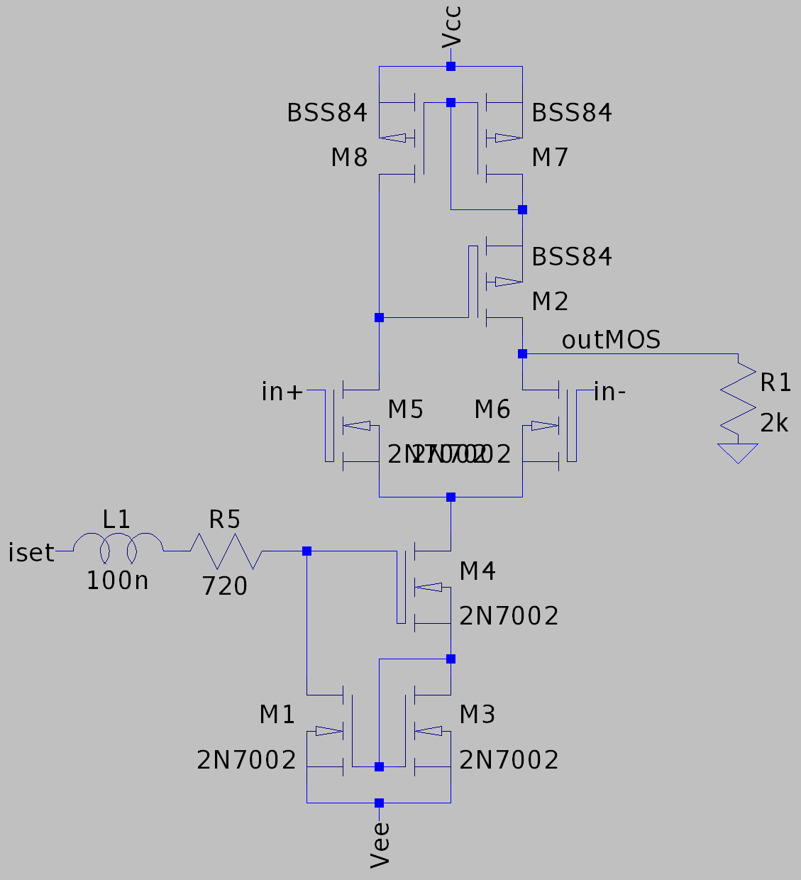
Ok nice, we have the same circuit, but with mosfets. But what’s going on with those other components ?
R1 is the output resistor. As you now know, an OTA’s output is a current, not a voltage, but for our application we need a voltage output, and a resistor just does that perfectly. You could get fancy with a transimpedance amplifier (the opposite of an OTA) but a resistor works great.
L1 and R5 together form a low-pass filter for the bias current. I don’t know why I picked L so low (-3dB at ~1GHz, big deal), feel free to do better. R5 alone allows the bias current to be driven by a voltage source, which makes the integration easier (here, with a ±5V source, the bias varies from 0 to ~10mA). If you want to keep a purely current-controlled bias, just put 0-ohms here instead. And remove the inductor.
Now you may wonder why I didn’t choose the ideal model for these transistors, and the answer is: it’s better to know that it’s working with imperfect, readily available components, and that you can just put them on a breadboard to really test everything if you want, with ideally no difference with the model.
You bet it does !
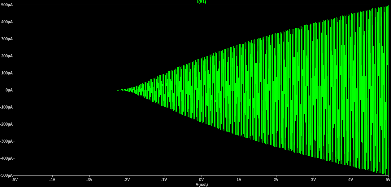
Feeding a ±15mV sine wave on the input, we get a nice ±500µA output with an iset voltage of +5V, and ±1,2nA at -5V, giving us a ~112dB dynamic range. I didn’t run the simulation for other supply voltages, as that’s what my preamp will run on, but I imagine larger supply would give a better dynamic range. Compared to the 30dB from the LM13700 typical application, it’s actually a huge improvement !
However, the input stage still saturates quite fast, hence the low amplitude of the input signal. This may be a problem regarding noise, so you need to be careful while routing your PCBs.
Also the bias’ voltage-to-current ratio is non linear, mostly because of the high bias current used here (~9mA). Lowering it will improve the linearity on this part, but increase the distortion on the main signal. And in an audio application, you probably won’t care if the volume knob isn’t perfectly logarithmic :p .
Well I dunno, I haven’t got my breadboards and transistors with me to test it, but the simulations show an improved THD, from -60dB to -70dB. Also the output is centered around zero, with no offset whatsoever, no trimpot to trim on each circuit, and no complicated equations when it comes to voltage dividers.
However the supply noise rejection is still as horrible as with most OTAs, so decouple the fuck out of it !
Anyway, so I started kicading…
With circuits like these, a breadboard won’t actually do it justice, with its parasitic capacitances and inductances everywhere. The right way is testing it on a PCB. And of course I used KiCAD !
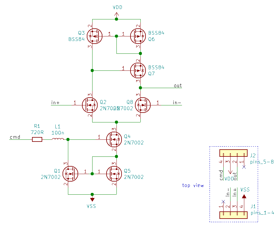
Same components, same circuit, but with added headers to plug the finished PCB into a breadboard or solder it onto another PCB. I chose to go with the standard single-opamp-on-8-pins pinout, and use the last unused pin for the bias setpoint (pins 1 and 5 are used as offset compensation on some opamps like the µA741). The schematic was the easy part, now to the routing…
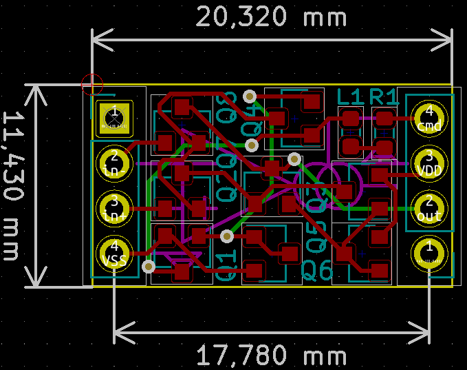
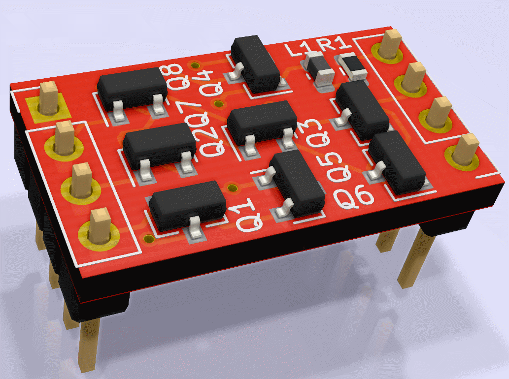
Heh it was actually quite easy too, took me around 1 hour as the components were very easy to place. I could even have gained a bit more width by placing all the transistors next to one another, maybe for revision 2. I even drew a little diagram on the bottom side, to prevent wiring errors on a breadboard !
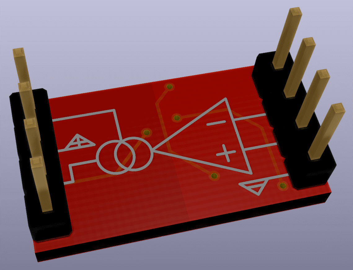
The headers can be soldered either way: on the diagram side like here, which makes it pin-compatible (but wider) with most opamps, or on the components side, which makes it breadboard-ready. Putting all the components on the bottom may lead to problems if you ever want to mount it flush on another PCB.
Gerber files: Revision 1; Revision 2
EDIT: I just realized that using packages with 2 transistors in them, I could gain a lot of space on the board, making it up to 5.08mm shorter ! Thus it would go from 0,7” pitch to 0,5” ! And if I drop the diagram side and fill it with components, I might even get it to fit on a standard DIP8 socket !
EDIT 2: I didn't have much free time in the last few weeks, so the revision 2 is just 0.1" shorter in both directions... But hey, that's still an improvement.